lmx2594 HDL worker
Warning
CRITICAL WARNING:
This HDL Worker will be relocated to opencpi/projects/platform/hdl/devices to best support component reuse.
Device Worker for the Texas Instruments LMX2594 15-GHz Wideband PLLATINUM(TM) RF Synthesizer
Detail
Register Properties
The raw properties corresponding to the LMX2594 registers are directly connected to the rawprops interface. This is required to be connected to a separate SPI primitive that converts memory mapped reads and writes of the raw properties to SPI transfers to the device.
The spi_lmx2594.vhd is a modified version of the framework supplied ./core/hdl/primitives/util/spi.vhd. Modifications were made to the spi.vhd to satisfy the timing diagrams that are listed in the device data-sheet which are also provided below.
While property paramaters build-time configuration of the SPI clock rate and the Control Plane clock, only one configuration has been validated on hardware.
All 113 device registers are defined as type ushort.
Registers R0 - R106:
volatileandwritableRegisters 107 - 112:
volatileonly.
Due to the nature of ushort register types, the props_in.raw.byte_enable signal needed to be used. The props_in.raw.byte_enable is included when a raw property is less than 32 bits. The (4) byte enables for reading/writing bytes in the 32-bit data path of the control interface.
Device Initialization Sequence
The lmx2594 device worker must adhere to the Recommended Initial Power-Up Sequence provided by the datasheet. The Device Initialization sequence will be provided here for reference:
Apply power to the device.
Program RESET = 1 to reset registers.
Program RESET = 0 to remove reset.
Program registers as shown in the register map in REVERSE order from highest to lowest.
Wait 10 ms.
Program register R0 one additional time with FCAL_EN = 1 to ensure that the VCO calibration runs from a stable state.
Block-Diagram
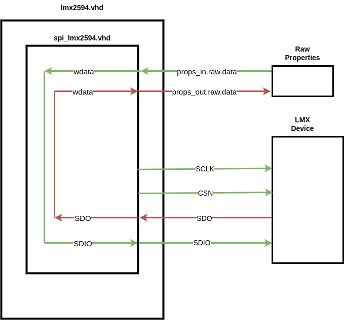
Control Timing and Signals
The device worker operates entirely in the control plane clock domain. All of the SPI signals are generated in the control plane domain.
Serial Data Input Timing Diagram:
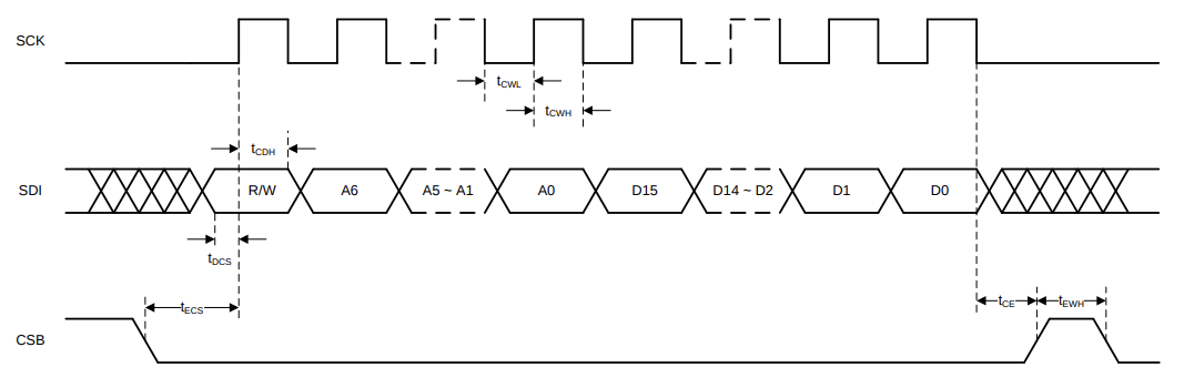
Write: R/W bit must be set to 0.
SDI: The data on SDI pin is clocked into a shift register on each rising edge on the SCK pin.
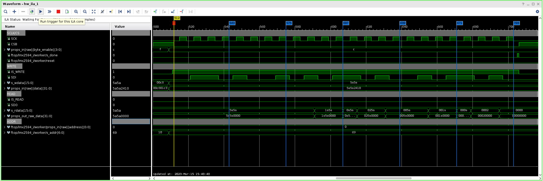
ILA Write Waveform:
ocpihdl set 3 register_105 0x5A5A
Serial Data Readback Timing Diagram:
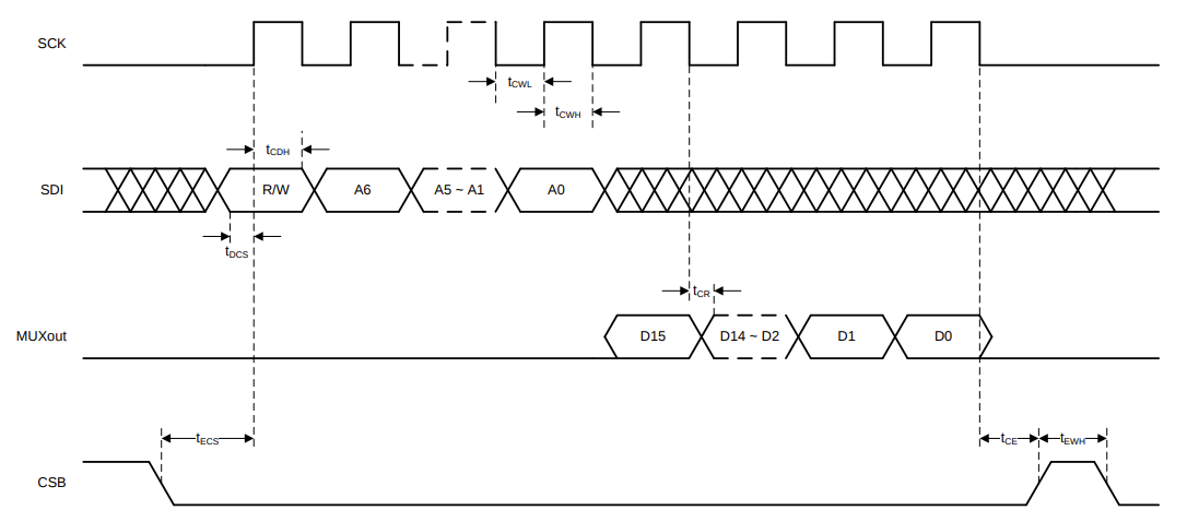
READ: R/W bit must be set to 1.
SDO/MUXout: The data on SDO/MUXout pin is clocked into a shift register on each falling edge on the SCK pin.
SDI: The data portion of the transition on the SDI line is always ignored.
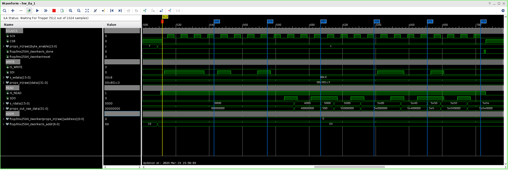
ILA Read Waveform
ocpihdl get 3 register_105