DRC FSM (fsmTesting)
Description
Verification application for the n310 Digital Radio Controller (drc_n310.rcc):
Finite State Machine (FSM) Operations
Channel Configuration
Platform Deployment
Build
Build the following components using the
ocpidev build --hdl-plaform n310within each component directory (./components).ocpi.osp.n3xx.portterm_csts
Build the following assemblies using
ocpidev build --hdl-plaform n310within each assemblies directory (./hdl/assemblies):fsmtesting
Build the application using
ocpidev build --rcc-platform ettus_n310_v4within the application directory. The application artifact is./target-ettus_n310_v4/fsmTesting.
Prerequisites
Copy DRC artifact into the OpenCPI artifacts directory (
/home/root/opencpi/artifacts) on then310platform:ocpi.osp.n3xx.devices.drc_n310.rcc.0.ettus_n310_v4.so
Copy the OAS file and ACI program into the application working directory on the
n310platform:fsmTesting.xml
target-ettus_n310_v4/fsmTesting
Execution
Run the application on the n310 platform:
% ./fsmTesting


Select test scenario to run for the DRC Application Tests
0       FSM Tests
1   Application Tests
>
FSM Tests
Used to verify the Finite-State Machine (FSM) operations for an OpenCPI Digital Radio Control (DRC). The n310 DRC (drc_n310.rcc) is based on the following FSM diagram:
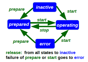
Figure 1: DRC FSM Diagram
Additonal logic is implemented into drc_n310.rcc to ensure compliance with the specification as defined in OpenCPI v2.4.3. The following test cases can be executed:
Select test scenario to run for the DRC FSM Application
        0       FSM Tests
        1       Application Tests
> 0

Select specific test to run for requested category (FSM Tests)
        0       prepare x2, start x2, stop x2, release x2
        1       start, stop release
        2       stop
        3       rf_port_num vs T/RX port constraint failure
        4       redundant rf_port_num channels configured
        5       Tolerance Failure -- tuning frequency
        6       Tolerance Failure -- RF Bandwidth
        7       Tolerance Failure -- Gain
        8       Daul Channel Type Deployment
>
FSM Tests Outputs
Case 0 - 1: Normal Operation for the configuration and deployment of an OpenCPI Channel Configuration on the
n310platform.
For Case 0, the application attempts to run the same FSM operation twice; however, drc_n310.rcc does not execute the operation per specification.For Case 1, the application executes the START operation from the INACTIVE state, which verifies drc_n310.rcc executes PREPARE operation before the START operation. A common output for a channel deployment is as follows:
config 0 State = inactive
OCPI( 3:580.0251): drc_n310: DBA:
Power Off Reset Control
-----------------------
CHIP            | POR
-----------------------
CPLD Pathing    | x
LMK04828        | x
ADF4351         | x
DSA             | x
CPLD GPIO POR   | x
Transceiver Obj | x
-----------------------
OCPI( 3:581.0636): drc_n310: DBA lmkController: PLLs locked
OCPI( 3:581.0637): drc_n310: DBA lmkController: SYNC Event
OCPI( 3:581.0686): drc_n310: DBA Transceiver: rx_clkgen: MMCM-PLL locked
OCPI( 3:581.0706): drc_n310: DBA Transceiver: tx_clkgen: MMCM-PLL locked
OCPI( 3:582.0476): drc_n310: DBA Transceiver: MCS successful
OCPI( 3:582.0477): drc_n310: DBA Transceiver: CLKPLL locked
OCPI( 3:587.0020): drc_n310: DBA Transceiver: AD9371 ARM version 5.2.2
OCPI( 3:587.0236): drc_n310: DBA Transceiver: PLLs locked
OCPI( 3:587.0256): drc_n310: DBA Transceiver: waiting for initCals (or 60 second timer)
OCPI( 3:592.0135): drc_n310: DBA Transceiver: Calibrations completed successfully
OCPI( 3:592.0256): drc_n310: DBA Transceiver: tx_adxcvr: OK
OCPI( 3:592.0376): drc_n310: DBA Transceiver: rx_adxcvr: OK
OCPI( 3:592.0387): drc_n310: DBA Transceiver: rx_jesd status:
        Link is enabled
        Measured Link Clock: 48.000 MHz
        Reported Link Clock: 48.000 MHz
        Lane rate: 1920.000 MHz
        Lane rate / 40: 48.000 MHz
        Link status: DATA
        SYSREF captured: Yes
        SYSREF alignment error: No
OCPI( 3:592.0392): drc_n310: DBA Transceiver: rx_jesd lane 0 status:
Errors: 1
        CGS state: DATA
        Initial Frame Synchronization: Yes
        Lane Latency: 2 Multi-frames and 15 Octets
        Initial Lane Alignment Sequence: Yes
        DID: 0, BID: 0, LID: 0, L: 4, SCR: 1, F: 2
        K: 32, M: 4, N: 16, CS: 0, N': 16, S: 1, HD: 0
        FCHK: 0x47, CF: 0
        ADJCNT: 0, PHADJ: 0, ADJDIR: 0, JESDV: 1, SUBCLASS: 1
        FC: 1920000 kHz
OCPI( 3:592.0398): drc_n310: DBA Transceiver: rx_jesd lane 1 status:
Errors: 1
        CGS state: DATA
        Initial Frame Synchronization: Yes
        Lane Latency: 2 Multi-frames and 55 Octets
        Initial Lane Alignment Sequence: Yes
        DID: 0, BID: 0, LID: 1, L: 4, SCR: 1, F: 2
        K: 32, M: 4, N: 16, CS: 0, N': 16, S: 1, HD: 0
        FCHK: 0x48, CF: 0
        ADJCNT: 0, PHADJ: 0, ADJDIR: 0, JESDV: 1, SUBCLASS: 1
        FC: 1920000 kHz
OCPI( 3:592.0402): drc_n310: DBA Transceiver: rx_jesd lane 2 status:
Errors: 1
        CGS state: DATA
        Initial Frame Synchronization: Yes
        Lane Latency: 2 Multi-frames and 43 Octets
        Initial Lane Alignment Sequence: Yes
        DID: 0, BID: 0, LID: 2, L: 4, SCR: 1, F: 2
        K: 32, M: 4, N: 16, CS: 0, N': 16, S: 1, HD: 0
        FCHK: 0x49, CF: 0
        ADJCNT: 0, PHADJ: 0, ADJDIR: 0, JESDV: 1, SUBCLASS: 1
        FC: 1920000 kHz
OCPI( 3:592.0405): drc_n310: DBA Transceiver: rx_jesd lane 3 status:
Errors: 0
        CGS state: DATA
        Initial Frame Synchronization: Yes
        Lane Latency: 2 Multi-frames and 1 Octets
        Initial Lane Alignment Sequence: Yes
        DID: 0, BID: 0, LID: 3, L: 4, SCR: 1, F: 2
        K: 32, M: 4, N: 16, CS: 0, N': 16, S: 1, HD: 0
        FCHK: 0x4A, CF: 0
        ADJCNT: 0, PHADJ: 0, ADJDIR: 0, JESDV: 1, SUBCLASS: 1
        FC: 1920000 kHz
OCPI( 3:592.0516): drc_n310: DBA Transceiver: rx_adc: Successfully initialized
OCPI( 3:592.0517): drc_n310: DBA Transceiver: tx_jesd status:
        Link is enabled
        Measured Link Clock: 48.000 MHz
        Reported Link Clock: 48.000 MHz
        Lane rate: 1920.000 MHz
        Lane rate / 40: 48.000 MHz
        SYNC~: deasserted
        Link status: DATA
        SYSREF captured: Yes
        SYSREF alignment error: No
OCPI( 3:592.0627): drc_n310: DBA Transceiver: tx_dac: Successfully initialized
OCPI( 3:592.0628): drc_n310: DBA Transceiver: Successful configuration of ad9371 chip
OCPI( 3:593.0289): drc_n310: prepare_config():
Upgraded config 0 from inactive state to prepared
config 0 State = prepared
config 0 State = prepared
OCPI( 3:593.0402): drc_n310: DBA: update_tuning_frequency bypassed due to parameter remaining unchanged
OCPI( 3:593.0726): drc_n310: DBA Transceiver: PLLs locked
OCPI( 3:593.0736): drc_n310: DBA Transceiver: waiting for initCals (or 60 second timer)
OCPI( 3:598.0335): drc_n310: DBA Transceiver: Calibrations completed successfully
OCPI( 3:599.0766): drc_n310: start_config():
Upgraded config 0 from prepared state to OPERATING state
config 0 State = operating
config 0 State = operating
OCPI( 3:599.0886): drc_n310: stop_config():
Downgraded from operating state to PREPARED state
config 0 State = prepared
config 0 State = prepared
OCPI( 3:599.0902): drc_n310: DBA Transceiver: rx_jesd status:
        Link is disabled
        Measured Link Clock: 48.000 MHz
        Reported Link Clock: 48.000 MHz
        External reset is deasserted
OCPI( 3:599.0906): drc_n310: DBA Transceiver: tx_jesd status:
        Link is disabled
        Measured Link Clock: 48.000 MHz
        Reported Link Clock: 48.000 MHz
        External reset is deasserted
OCPI( 3:599.0909): drc_n310: DBA:
Power Off Reset Control
-----------------------
CHIP            | POR
-----------------------
CPLD Pathing    | x
LMK04828        | x
ADF4351         | x
DSA             |
CPLD GPIO POR   | x
Transceiver Obj | x
-----------------------
OCPI( 3:599.0922): drc_n310: DBB:
Power Off Reset Control
-----------------------
CHIP            | POR
-----------------------
CPLD Pathing    | x
LMK04828        | x
ADF4351         | x
DSA             | x
CPLD GPIO POR   | x
Transceiver Obj | x
-----------------------
OCPI( 3:599.0927): drc_n310: release_config():
Downgraded config 0 from prepared state to inactive state
config 0 State = inactive
OCPI( 3:599.0929): drc_n310: DBA:
Power Off Reset Control
-----------------------
CHIP            | POR
-----------------------
CPLD Pathing    |
LMK04828        |
ADF4351         |
DSA             |
CPLD GPIO POR   |
Transceiver Obj |
-----------------------
OCPI( 3:599.0933): drc_n310: DBB:
Power Off Reset Control
-----------------------
CHIP            | POR
-----------------------
CPLD Pathing    |
LMK04828        |
ADF4351         |
DSA             |
CPLD GPIO POR   |
Transceiver Obj |
-----------------------
OCPI( 3:599.0934): drc_n310: release_config():
Downgraded config 0 from inactive state to inactive state
config 0 State = inactive
OCPI( 3:599.0940): drc_n310: DBA:
Power Off Reset Control
-----------------------
CHIP            | POR
-----------------------
CPLD Pathing    |
LMK04828        |
ADF4351         |
DSA             |
CPLD GPIO POR   |
Transceiver Obj |
-----------------------
OCPI( 3:599.0940): drc_n310: DBB:
Power Off Reset Control
-----------------------
CHIP            | POR
-----------------------
CPLD Pathing    |
LMK04828        |
ADF4351         |
DSA             |
CPLD GPIO POR   |
Transceiver Obj |
-----------------------
OCPI( 3:599.0941): drc_n310: release_config():
Downgraded config 0 from inactive state to inactive state
Case 2: The application executes the STOP operation from the INACTIVE state, which is not a valid operation for the INACTIVE state. As a result,
drc_n310.ccreturns RCC_ERROR, which should place the FSM into the ERROR state. However, the OpenCPI Framework failed to place the DRC into the ERROR state. The developers have an issue open with the OpenCPI Framework team to address this bug. The output is as follows:
config 0 State = inactive
App Stop with nothing else causes exception assert.
config 0 State = prepared
fsmTesting: fsmTesting.cc:1479: bool drc_n310_testing_suite(OCPI:API::Property&, OCPI::API::Application&, testSelection&):Assertion     `stateHelper.at(_stateHelper::inactive)==getConfigState(app,0)' failed.
Aborted
Case 3 -7: Verification tests to ensure that
drc_n310.rccperform the required checks for deploying an OpenCPI Channel Configuration. During the PREPARE operation,drc_n310.rccperforms various configuration and tolerance checks. Failure to meet the checks, ``drc_n310``returns RCC_ERROR. As a result, the FSM should be placed in the ERROR state. However, the OpenCPI Framework failed to place the DRC into the ERROR state. The developers have an issue open with the OpenCPI Framework team to address this bug. A similar output will occur as follows:
config 0 State = inactive
OCPI( 3:518.0814): drc_n310: DBA:
Power Off Reset Control
-----------------------
CHIP            | POR
-----------------------
CPLD Pathing    | x
LMK04828        | x
ADF4351         | x
DSA             | x
CPLD GPIO POR   | x
Transceiver Obj | x
-----------------------
OCPI( 3:520.0906): drc_n310: DBA lmkController: PLLs locked
OCPI( 3:520.0906): drc_n310: DBA lmkController: SYNC Event
OCPI( 3:520.0956): drc_n310: DBA Transceiver: rx_clkgen: MMCM-PLL locked
OCPI( 3:520.0976): drc_n310: DBA Transceiver: tx_clkgen: MMCM-PLL locked
OCPI( 3:521.0746): drc_n310: DBA Transceiver: MCS successful
OCPI( 3:521.0746): drc_n310: DBA Transceiver: CLKPLL locked
OCPI( 3:526.0100): drc_n310: DBA Transceiver: AD9371 ARM version 5.2.2
OCPI( 3:526.0426): drc_n310: DBA Transceiver: PLLs locked
OCPI( 3:526.0439): drc_n310: DBA Transceiver: waiting for initCals (or 60 second timer)
OCPI( 3:531.0318): drc_n310: DBA Transceiver: Calibrations completed successfully
OCPI( 3:531.0436): drc_n310: DBA Transceiver: tx_adxcvr: OK
OCPI( 3:531.0556): drc_n310: DBA Transceiver: rx_adxcvr: OK
OCPI( 3:531.0566): drc_n310: DBA Transceiver: rx_jesd status:
        Link is enabled
        Measured Link Clock: 48.000 MHz
        Reported Link Clock: 48.000 MHz
        Lane rate: 1920.000 MHz
        Lane rate / 40: 48.000 MHz
        Link status: DATA
        SYSREF captured: Yes
        SYSREF alignment error: No
OCPI( 3:531.0572): drc_n310: DBA Transceiver: rx_jesd lane 0 status:
Errors: 1
        CGS state: DATA
        Initial Frame Synchronization: Yes
        Lane Latency: 2 Multi-frames and 28 Octets
        Initial Lane Alignment Sequence: Yes
        DID: 0, BID: 0, LID: 0, L: 4, SCR: 1, F: 2
        K: 32, M: 4, N: 16, CS: 0, N': 16, S: 1, HD: 0
        FCHK: 0x47, CF: 0
        ADJCNT: 0, PHADJ: 0, ADJDIR: 0, JESDV: 1, SUBCLASS: 1
        FC: 1920000 kHz
OCPI( 3:531.0577): drc_n310: DBA Transceiver: rx_jesd lane 1 status:
Errors: 0
        CGS state: DATA
        Initial Frame Synchronization: Yes
        Lane Latency: 2 Multi-frames and 12 Octets
        Initial Lane Alignment Sequence: Yes
        DID: 0, BID: 0, LID: 1, L: 4, SCR: 1, F: 2
        K: 32, M: 4, N: 16, CS: 0, N': 16, S: 1, HD: 0
        FCHK: 0x48, CF: 0
        ADJCNT: 0, PHADJ: 0, ADJDIR: 0, JESDV: 1, SUBCLASS: 1
        FC: 1920000 kHz
OCPI( 3:531.0581): drc_n310: DBA Transceiver: rx_jesd lane 2 status:
Errors: 0
        CGS state: DATA
        Initial Frame Synchronization: Yes
        Lane Latency: 1 Multi-frames and 58 Octets
        Initial Lane Alignment Sequence: Yes
        DID: 0, BID: 0, LID: 2, L: 4, SCR: 1, F: 2
        K: 32, M: 4, N: 16, CS: 0, N': 16, S: 1, HD: 0
        FCHK: 0x49, CF: 0
        ADJCNT: 0, PHADJ: 0, ADJDIR: 0, JESDV: 1, SUBCLASS: 1
        FC: 1920000 kHz
OCPI( 3:531.0584): drc_n310: DBA Transceiver: rx_jesd lane 3 status:
Errors: 0
        CGS state: DATA
        Initial Frame Synchronization: Yes
        Lane Latency: 2 Multi-frames and 0 Octets
        Initial Lane Alignment Sequence: Yes
        DID: 0, BID: 0, LID: 3, L: 4, SCR: 1, F: 2
        K: 32, M: 4, N: 16, CS: 0, N': 16, S: 1, HD: 0
        FCHK: 0x4A, CF: 0
        ADJCNT: 0, PHADJ: 0, ADJDIR: 0, JESDV: 1, SUBCLASS: 1
        FC: 1920000 kHz
OCPI( 3:531.0696): drc_n310: DBA Transceiver: rx_adc: Successfully initialized
OCPI( 3:531.0697): drc_n310: DBA Transceiver: tx_jesd status:
        Link is enabled
        Measured Link Clock: 48.000 MHz
        Reported Link Clock: 48.000 MHz
        Lane rate: 1920.000 MHz
        Lane rate / 40: 48.000 MHz
        SYNC~: deasserted
        Link status: DATA
        SYSREF captured: Yes
        SYSREF alignment error: No
OCPI( 3:531.0806): drc_n310: DBA Transceiver: tx_dac: Successfully initialized
OCPI( 3:531.0807): drc_n310: DBA Transceiver: Successful configuration of ad9371 chip
OCPI( 3:532.0478): drc_n310: DBA: validateChannelConfig(): db_port_num=0
Failed tolerance_tuning_freq_MHz check:
        Programmed value: 10
        Requested value: 8
        Defined Tolerance: 1
OCPI( 3:532.0481): drc_n310: prepare_config():
DBA failed to properly configure its profile
config 0 State = inactive
fsmTesting: fsmTesting.cc:1506: bool drc_n310_testing_suite(OCPI::API::Property&, OCPI::API::Application&, testSelection&): Assertion   `stateHelper.at(_stateHelper::error)==getConfigState(app,0)' failed.
Aborted
Case 8: Checks the configuration and tolerances for a dual channel type deployment onto a single daughterboard. Several parameters are linked for the configuration of the AD9371 transceiver. This test demonstrates the deployment onto the
n310platform. The output is as follows:
config 0 State = inactive
OCPI( 3: 25.0081): drc_n310: DBA:
Power Off Reset Control
-----------------------
CHIP            | POR
-----------------------
CPLD Pathing    | x
LMK04828        | x
ADF4351         | x
DSA             | x
CPLD GPIO POR   | x
Transceiver Obj | x
-----------------------
OCPI( 3: 25.0866): drc_n310: DBA lmkController: PLLs locked
OCPI( 3: 25.0867): drc_n310: DBA lmkController: SYNC Event
OCPI( 3: 25.0896): drc_n310: DBA Transceiver: rx_clkgen: MMCM-PLL locked
OCPI( 3: 26.0656): drc_n310: DBA Transceiver: MCS successful
OCPI( 3: 26.0657): drc_n310: DBA Transceiver: CLKPLL locked
OCPI( 3: 30.0343): drc_n310: DBA Transceiver: AD9371 ARM version 5.2.2
OCPI( 3: 30.0666): drc_n310: DBA Transceiver: PLLs locked
OCPI( 3: 30.0686): drc_n310: DBA Transceiver: waiting for initCals (or 60 second timer)
OCPI( 3: 35.0619): drc_n310: DBA Transceiver: Calibrations completed successfully
OCPI( 3: 35.0736): drc_n310: DBA Transceiver: rx_adxcvr: OK
OCPI( 3: 35.0747): drc_n310: DBA Transceiver: rx_jesd status:
        Link is enabled
        Measured Link Clock: 48.000 MHz
        Reported Link Clock: 48.000 MHz
        Lane rate: 1920.000 MHz
        Lane rate / 40: 48.000 MHz
        Link status: DATA
        SYSREF captured: Yes
        SYSREF alignment error: No
OCPI( 3: 35.0752): drc_n310: DBA Transceiver: rx_jesd lane 0 status:
Errors: 0
        CGS state: DATA
        Initial Frame Synchronization: Yes
        Lane Latency: 1 Multi-frames and 61 Octets
        Initial Lane Alignment Sequence: Yes
        DID: 0, BID: 0, LID: 0, L: 4, SCR: 1, F: 2
        K: 32, M: 4, N: 16, CS: 0, N': 16, S: 1, HD: 0
        FCHK: 0x47, CF: 0
        ADJCNT: 0, PHADJ: 0, ADJDIR: 0, JESDV: 1, SUBCLASS: 1
        FC: 1920000 kHz
OCPI( 3: 35.0758): drc_n310: DBA Transceiver: rx_jesd lane 1 status:
Errors: 0
        CGS state: DATA
        Initial Frame Synchronization: Yes
        Lane Latency: 1 Multi-frames and 59 Octets
        Initial Lane Alignment Sequence: Yes
        DID: 0, BID: 0, LID: 1, L: 4, SCR: 1, F: 2
        K: 32, M: 4, N: 16, CS: 0, N': 16, S: 1, HD: 0
        FCHK: 0x48, CF: 0
        ADJCNT: 0, PHADJ: 0, ADJDIR: 0, JESDV: 1, SUBCLASS: 1
        FC: 1920000 kHz
OCPI( 3: 35.0761): drc_n310: DBA Transceiver: rx_jesd lane 2 status:
Errors: 1
        CGS state: DATA
        Initial Frame Synchronization: Yes
        Lane Latency: 2 Multi-frames and 49 Octets
        Initial Lane Alignment Sequence: Yes
        DID: 0, BID: 0, LID: 2, L: 4, SCR: 1, F: 2
        K: 32, M: 4, N: 16, CS: 0, N': 16, S: 1, HD: 0
        FCHK: 0x49, CF: 0
        ADJCNT: 0, PHADJ: 0, ADJDIR: 0, JESDV: 1, SUBCLASS: 1
        FC: 1920000 kHz
OCPI( 3: 35.0764): drc_n310: DBA Transceiver: rx_jesd lane 3 status:
Errors: 1
        CGS state: DATA
        Initial Frame Synchronization: Yes
        Lane Latency: 2 Multi-frames and 3 Octets
        Initial Lane Alignment Sequence: Yes
        DID: 0, BID: 0, LID: 3, L: 4, SCR: 1, F: 2
        K: 32, M: 4, N: 16, CS: 0, N': 16, S: 1, HD: 0
        FCHK: 0x4A, CF: 0
        ADJCNT: 0, PHADJ: 0, ADJDIR: 0, JESDV: 1, SUBCLASS: 1
        FC: 1920000 kHz
OCPI( 3: 35.0876): drc_n310: DBA Transceiver: rx_adc: Successfully initialized
OCPI( 3: 35.0877): drc_n310: DBA Transceiver: Successful configuration of ad9371 chip
OCPI( 3: 36.0718): drc_n310: DBA: validateChannelConfig(): db_port_num=3
Failed tolerance_tuning_freq_MHz check:
        Programmed value: 380
        Requested value: 670
        Defined Tolerance: 0.01
OCPI( 3: 36.0721): drc_n310: prepare_config():
DBA failed to properly configure its profile
config 0 State = inactive
OCPI( 3: 36.0731): drc_n310: DBA Transceiver: rx_jesd status:
        Link is disabled
        Measured Link Clock: 48.000 MHz
        Reported Link Clock: 48.000 MHz
        External reset is deasserted
OCPI( 3: 36.0733): drc_n310: DBA:
Power Off Reset Control
-----------------------
CHIP            | POR
-----------------------
CPLD Pathing    | x
LMK04828        | x
ADF4351         |
DSA             |
CPLD GPIO POR   |
Transceiver Obj | x
-----------------------
OCPI( 3: 37.0756): drc_n310: DBA lmkController: PLLs locked
OCPI( 3: 37.0757): drc_n310: DBA lmkController: SYNC Event
OCPI( 3: 37.0786): drc_n310: DBA Transceiver: rx_clkgen: MMCM-PLL locked
OCPI( 3: 38.0546): drc_n310: DBA Transceiver: MCS successful
OCPI( 3: 38.0547): drc_n310: DBA Transceiver: CLKPLL locked
OCPI( 3: 43.0310): drc_n310: DBA Transceiver: AD9371 ARM version 5.2.2
OCPI( 3: 43.0526): drc_n310: DBA Transceiver: PLLs locked
OCPI( 3: 43.0546): drc_n310: DBA Transceiver: waiting for initCals (or 60 second timer)
OCPI( 3: 48.0480): drc_n310: DBA Transceiver: Calibrations completed successfully
OCPI( 3: 48.0596): drc_n310: DBA Transceiver: rx_adxcvr: OK
OCPI( 3: 48.0607): drc_n310: DBA Transceiver: rx_jesd status:
        Link is enabled
        Measured Link Clock: 48.000 MHz
        Reported Link Clock: 48.000 MHz
        Lane rate: 1920.000 MHz
        Lane rate / 40: 48.000 MHz
        Link status: DATA
        SYSREF captured: Yes
        SYSREF alignment error: No
OCPI( 3: 48.0612): drc_n310: DBA Transceiver: rx_jesd lane 0 status:
Errors: 1
        CGS state: DATA
        Initial Frame Synchronization: Yes
        Lane Latency: 1 Multi-frames and 62 Octets
        Initial Lane Alignment Sequence: Yes
        DID: 0, BID: 0, LID: 0, L: 4, SCR: 1, F: 2
        K: 32, M: 4, N: 16, CS: 0, N': 16, S: 1, HD: 0
        FCHK: 0x47, CF: 0
        ADJCNT: 0, PHADJ: 0, ADJDIR: 0, JESDV: 1, SUBCLASS: 1
        FC: 1920000 kHz
OCPI( 3: 48.0618): drc_n310: DBA Transceiver: rx_jesd lane 1 status:
Errors: 0
        CGS state: DATA
        Initial Frame Synchronization: Yes
        Lane Latency: 2 Multi-frames and 50 Octets
        Initial Lane Alignment Sequence: Yes
        DID: 0, BID: 0, LID: 1, L: 4, SCR: 1, F: 2
        K: 32, M: 4, N: 16, CS: 0, N': 16, S: 1, HD: 0
        FCHK: 0x48, CF: 0
        ADJCNT: 0, PHADJ: 0, ADJDIR: 0, JESDV: 1, SUBCLASS: 1
        FC: 1920000 kHz
OCPI( 3: 48.0621): drc_n310: DBA Transceiver: rx_jesd lane 2 status:
Errors: 1
        CGS state: DATA
        Initial Frame Synchronization: Yes
        Lane Latency: 2 Multi-frames and 30 Octets
        Initial Lane Alignment Sequence: Yes
        DID: 0, BID: 0, LID: 2, L: 4, SCR: 1, F: 2
        K: 32, M: 4, N: 16, CS: 0, N': 16, S: 1, HD: 0
        FCHK: 0x49, CF: 0
        ADJCNT: 0, PHADJ: 0, ADJDIR: 0, JESDV: 1, SUBCLASS: 1
        FC: 1920000 kHz
OCPI( 3: 48.0624): drc_n310: DBA Transceiver: rx_jesd lane 3 status:
Errors: 0
        CGS state: DATA
        Initial Frame Synchronization: Yes
        Lane Latency: 2 Multi-frames and 0 Octets
        Initial Lane Alignment Sequence: Yes
        DID: 0, BID: 0, LID: 3, L: 4, SCR: 1, F: 2
        K: 32, M: 4, N: 16, CS: 0, N': 16, S: 1, HD: 0
        FCHK: 0x4A, CF: 0
        ADJCNT: 0, PHADJ: 0, ADJDIR: 0, JESDV: 1, SUBCLASS: 1
        FC: 1920000 kHz
OCPI( 3: 48.0736): drc_n310: DBA Transceiver: rx_adc: Successfully initialized
OCPI( 3: 48.0737): drc_n310: DBA Transceiver: Successful configuration of ad9371 chip
OCPI( 3: 49.0578): drc_n310: prepare_config():
Upgraded config 0 from inactive state to prepared
config 0 State = prepared
OCPI( 3: 49.0699): drc_n310: DBA: update_tuning_frequency bypassed due to parameter remaining unchanged
OCPI( 3: 49.0906): drc_n310: DBA Transceiver: PLLs locked
OCPI( 3: 49.0916): drc_n310: DBA Transceiver: waiting for initCals (or 60 second timer)
OCPI( 3: 51.0301): drc_n310: DBA Transceiver: Calibrations completed successfully
OCPI( 3: 55.0946): drc_n310: start_config():
Upgraded config 0 from prepared state to OPERATING state
config 0 State = operating
OCPI( 3: 55.0951): drc_n310: stop_config():
Downgraded from operating state to PREPARED state
config 0 State = prepared
OCPI( 3: 55.0963): drc_n310: DBA Transceiver: rx_jesd status:
        Link is disabled
        Measured Link Clock: 48.000 MHz
        Reported Link Clock: 48.000 MHz
        External reset is deasserted
OCPI( 3: 55.0965): drc_n310: DBA:
Power Off Reset Control
-----------------------
CHIP            | POR
-----------------------
CPLD Pathing    | x
LMK04828        | x
ADF4351         |
DSA             |
CPLD GPIO POR   | x
Transceiver Obj | x
-----------------------
OCPI( 3: 55.0978): drc_n310: DBB:
Power Off Reset Control
-----------------------
CHIP            | POR
-----------------------
CPLD Pathing    | x
LMK04828        | x
ADF4351         | x
DSA             | x
CPLD GPIO POR   | x
Transceiver Obj | x
-----------------------
OCPI( 3: 55.0983): drc_n310: release_config():
Downgraded config 0 from prepared state to inactive state
config 0 State = inactive
OCPI( 3: 55.0989): drc_n310: DBA:
Power Off Reset Control
-----------------------
CHIP            | POR
-----------------------
CPLD Pathing    |
LMK04828        |
ADF4351         |
DSA             |
CPLD GPIO POR   |
Transceiver Obj |
-----------------------
OCPI( 3: 55.0990): drc_n310: DBB:
Power Off Reset Control
-----------------------
CHIP            | POR
-----------------------
CPLD Pathing    |
LMK04828        |
ADF4351         |
DSA             |
CPLD GPIO POR   |
Transceiver Obj |
-----------------------
OCPI( 3: 55.0991): drc_n310: release_config():
Downgraded config 0 from inactive state to inactive state
Application Tests
Used to verify OpenCPI channel configurations and deployment across the n310 platform:
Select test scenario to run for the DRC FSM Application
        0       FSM Tests
        1       Application Tests
> 1

Select specific test to run for requested category (Application Tests)
        0       DBA AND DBB - TX0 TX1 RX0 RX1  - 96 MHZ
        1       DBA         - TX0 RX1          - 96 MHZ
        2       DBB         - TX1 RX0          - 96 MHZ
        3       DBA         - TX0 TX1 RX0 RX1  - 90 MHZ
        4       DBB         - TX0 TX1 RX0 RX1  - 90 MHZ
        5       Toggle individual channels across both daughterboards
>
Application Tests Outputs
For each test case, the application will deploy the OpenCPI channel configuration based on the following rf_port_num mapping to n310 RF ports:

Figure 2: n310 DRC Channel Mapping
- DRC RF Port Number: 3-Bit Mapping
rf_port_num[2]: {0:DBA, 1:DBB} - Daughterboard (DB) Selection
rf_port_num[1]: {0:TX, 1:RX} - Channel Type
rf_port_num[0]: {0:CH0, 1:CH1} - Channel Selection
The channel deployment is verify by the RF Port LEDs on the ``n310`` platform during the running of the application. A common output for a channel deployment is as follows:
Select specific test to run for requested category (Application Tests)
        0       DBA AND DBB - TX0 TX1 RX0 RX1  - 96 MHZ
        1       DBA         - TX0 RX1          - 96 MHZ
        2       DBB         - TX1 RX0          - 96 MHZ
        3       DBA         - TX0 TX1 RX0 RX1  - 90 MHZ
        4       DBB         - TX0 TX1 RX0 RX1  - 90 MHZ
        5       Toggle individual channels across both daughterboards
> 0

config 0 State = inactive
OCPI( 3:431.0383): drc_n310: DBA:
Power Off Reset Control
-----------------------
CHIP            | POR
-----------------------
CPLD Pathing    | x
LMK04828        | x
ADF4351         | x
DSA             | x
CPLD GPIO POR   | x
Transceiver Obj | x
-----------------------
OCPI( 3:431.0919): drc_n310: DBA lmkController: PLLs locked
OCPI( 3:431.0920): drc_n310: DBA lmkController: SYNC Event
OCPI( 3:431.0969): drc_n310: DBA Transceiver: rx_clkgen: MMCM-PLL locked
OCPI( 3:431.0989): drc_n310: DBA Transceiver: tx_clkgen: MMCM-PLL locked
OCPI( 3:432.0759): drc_n310: DBA Transceiver: MCS successful
OCPI( 3:432.0760): drc_n310: DBA Transceiver: CLKPLL locked
OCPI( 3:437.0533): drc_n310: DBA Transceiver: AD9371 ARM version 5.2.2
OCPI( 3:437.0859): drc_n310: DBA Transceiver: PLLs locked
OCPI( 3:437.0880): drc_n310: DBA Transceiver: waiting for initCals (or 60 second timer)
OCPI( 3:442.0759): drc_n310: DBA Transceiver: Calibrations completed successfully
OCPI( 3:442.0879): drc_n310: DBA Transceiver: tx_adxcvr: OK
OCPI( 3:442.0999): drc_n310: DBA Transceiver: rx_adxcvr: OK
OCPI( 3:443.0010): drc_n310: DBA Transceiver: rx_jesd status:
        Link is enabled
        Measured Link Clock: 48.000 MHz
        Reported Link Clock: 48.000 MHz
        Lane rate: 1920.000 MHz
        Lane rate / 40: 48.000 MHz
        Link status: DATA
        SYSREF captured: Yes
        SYSREF alignment error: No
OCPI( 3:443.0015): drc_n310: DBA Transceiver: rx_jesd lane 0 status:
Errors: 1
        CGS state: DATA
        Initial Frame Synchronization: Yes
        Lane Latency: 2 Multi-frames and 10 Octets
        Initial Lane Alignment Sequence: Yes
        DID: 0, BID: 0, LID: 0, L: 4, SCR: 1, F: 2
        K: 32, M: 4, N: 16, CS: 0, N': 16, S: 1, HD: 0
        FCHK: 0x47, CF: 0
        ADJCNT: 0, PHADJ: 0, ADJDIR: 0, JESDV: 1, SUBCLASS: 1
        FC: 1920000 kHz
OCPI( 3:443.0021): drc_n310: DBA Transceiver: rx_jesd lane 1 status:
Errors: 0
        CGS state: DATA
        Initial Frame Synchronization: Yes
        Lane Latency: 2 Multi-frames and 50 Octets
        Initial Lane Alignment Sequence: Yes
        DID: 0, BID: 0, LID: 1, L: 4, SCR: 1, F: 2
        K: 32, M: 4, N: 16, CS: 0, N': 16, S: 1, HD: 0
        FCHK: 0x48, CF: 0
        ADJCNT: 0, PHADJ: 0, ADJDIR: 0, JESDV: 1, SUBCLASS: 1
        FC: 1920000 kHz
OCPI( 3:443.0025): drc_n310: DBA Transceiver: rx_jesd lane 2 status:
Errors: 1
        CGS state: DATA
        Initial Frame Synchronization: Yes
        Lane Latency: 2 Multi-frames and 46 Octets
        Initial Lane Alignment Sequence: Yes
        DID: 0, BID: 0, LID: 2, L: 4, SCR: 1, F: 2
        K: 32, M: 4, N: 16, CS: 0, N': 16, S: 1, HD: 0
        FCHK: 0x49, CF: 0
        ADJCNT: 0, PHADJ: 0, ADJDIR: 0, JESDV: 1, SUBCLASS: 1
        FC: 1920000 kHz
OCPI( 3:443.0027): drc_n310: DBA Transceiver: rx_jesd lane 3 status:
Errors: 0
        CGS state: DATA
        Initial Frame Synchronization: Yes
        Lane Latency: 2 Multi-frames and 2 Octets
        Initial Lane Alignment Sequence: Yes
        DID: 0, BID: 0, LID: 3, L: 4, SCR: 1, F: 2
        K: 32, M: 4, N: 16, CS: 0, N': 16, S: 1, HD: 0
        FCHK: 0x4A, CF: 0
        ADJCNT: 0, PHADJ: 0, ADJDIR: 0, JESDV: 1, SUBCLASS: 1
        FC: 1920000 kHz
OCPI( 3:443.0139): drc_n310: DBA Transceiver: rx_adc: Successfully initialized
OCPI( 3:443.0140): drc_n310: DBA Transceiver: tx_jesd status:
        Link is enabled
        Measured Link Clock: 48.000 MHz
        Reported Link Clock: 48.000 MHz
        Lane rate: 1920.000 MHz
        Lane rate / 40: 48.000 MHz
        SYNC~: deasserted
        Link status: DATA
        SYSREF captured: Yes
        SYSREF alignment error: No
OCPI( 3:443.0250): drc_n310: DBA Transceiver: tx_dac: Successfully initialized
OCPI( 3:443.0250): drc_n310: DBA Transceiver: Successful configuration of ad9371 chip
OCPI( 3:443.0933): drc_n310: DBB:
Power Off Reset Control
-----------------------
CHIP            | POR
-----------------------
CPLD Pathing    | x
LMK04828        | x
ADF4351         | x
DSA             | x
CPLD GPIO POR   | x
Transceiver Obj | x
-----------------------
OCPI( 3:444.0359): drc_n310: DBB lmkController: PLLs locked
OCPI( 3:444.0360): drc_n310: DBB lmkController: SYNC Event
OCPI( 3:444.0389): drc_n310: DBB Transceiver: rx_clkgen: MMCM-PLL locked
OCPI( 3:444.0409): drc_n310: DBB Transceiver: tx_clkgen: MMCM-PLL locked
OCPI( 3:445.0179): drc_n310: DBB Transceiver: MCS successful
OCPI( 3:445.0180): drc_n310: DBB Transceiver: CLKPLL locked
OCPI( 3:449.0843): drc_n310: DBB Transceiver: AD9371 ARM version 5.2.2
OCPI( 3:450.0060): drc_n310: DBB Transceiver: PLLs locked
OCPI( 3:450.0080): drc_n310: DBB Transceiver: waiting for initCals (or 60 second timer)
OCPI( 3:461.0438): drc_n310: DBB Transceiver: Calibrations completed successfully
OCPI( 3:461.0560): drc_n310: DBB Transceiver: tx_adxcvr: OK
OCPI( 3:461.0680): drc_n310: DBB Transceiver: rx_adxcvr: OK
OCPI( 3:461.0690): drc_n310: DBB Transceiver: rx_jesd status:
        Link is enabled
        Measured Link Clock: 48.000 MHz
        Reported Link Clock: 48.000 MHz
        Lane rate: 1920.000 MHz
        Lane rate / 40: 48.000 MHz
        Link status: DATA
        SYSREF captured: Yes
        SYSREF alignment error: No
OCPI( 3:461.0696): drc_n310: DBB Transceiver: rx_jesd lane 0 status:
Errors: 0
        CGS state: DATA
        Initial Frame Synchronization: Yes
        Lane Latency: 2 Multi-frames and 23 Octets
        Initial Lane Alignment Sequence: Yes
        DID: 0, BID: 0, LID: 0, L: 4, SCR: 1, F: 2
        K: 32, M: 4, N: 16, CS: 0, N': 16, S: 1, HD: 0
        FCHK: 0x47, CF: 0
        ADJCNT: 0, PHADJ: 0, ADJDIR: 0, JESDV: 1, SUBCLASS: 1
        FC: 1920000 kHz
OCPI( 3:461.0701): drc_n310: DBB Transceiver: rx_jesd lane 1 status:
Errors: 0
        CGS state: DATA
        Initial Frame Synchronization: Yes
        Lane Latency: 1 Multi-frames and 63 Octets
        Initial Lane Alignment Sequence: Yes
        DID: 0, BID: 0, LID: 1, L: 4, SCR: 1, F: 2
        K: 32, M: 4, N: 16, CS: 0, N': 16, S: 1, HD: 0
        FCHK: 0x48, CF: 0
        ADJCNT: 0, PHADJ: 0, ADJDIR: 0, JESDV: 1, SUBCLASS: 1
        FC: 1920000 kHz
OCPI( 3:461.0705): drc_n310: DBB Transceiver: rx_jesd lane 2 status:
Errors: 0
        CGS state: DATA
        Initial Frame Synchronization: Yes
        Lane Latency: 2 Multi-frames and 11 Octets
        Initial Lane Alignment Sequence: Yes
        DID: 0, BID: 0, LID: 2, L: 4, SCR: 1, F: 2
        K: 32, M: 4, N: 16, CS: 0, N': 16, S: 1, HD: 0
        FCHK: 0x49, CF: 0
        ADJCNT: 0, PHADJ: 0, ADJDIR: 0, JESDV: 1, SUBCLASS: 1
        FC: 1920000 kHz
OCPI( 3:461.0708): drc_n310: DBB Transceiver: rx_jesd lane 3 status:
Errors: 1
        CGS state: DATA
        Initial Frame Synchronization: Yes
        Lane Latency: 1 Multi-frames and 55 Octets
        Initial Lane Alignment Sequence: Yes
        DID: 0, BID: 0, LID: 3, L: 4, SCR: 1, F: 2
        K: 32, M: 4, N: 16, CS: 0, N': 16, S: 1, HD: 0
        FCHK: 0x4A, CF: 0
        ADJCNT: 0, PHADJ: 0, ADJDIR: 0, JESDV: 1, SUBCLASS: 1
        FC: 1920000 kHz
OCPI( 3:461.0820): drc_n310: DBB Transceiver: rx_adc: Successfully initialized
OCPI( 3:461.0821): drc_n310: DBB Transceiver: tx_jesd status:
        Link is enabled
        Measured Link Clock: 48.000 MHz
        Reported Link Clock: 48.000 MHz
        Lane rate: 1920.000 MHz
        Lane rate / 40: 48.000 MHz
        SYNC~: deasserted
        Link status: DATA
        SYSREF captured: Yes
        SYSREF alignment error: No
OCPI( 3:461.0930): drc_n310: DBB Transceiver: tx_dac: Successfully initialized
OCPI( 3:461.0931): drc_n310: DBB Transceiver: Successful configuration of ad9371 chip
OCPI( 3:462.0124): drc_n310: prepare_config():
Upgraded config 0 from inactive state to prepared
config 0 State = prepared
OCPI( 3:462.0249): drc_n310: DBA: update_tuning_frequency bypassed due to parameter remaining unchanged
OCPI( 3:462.0570): drc_n310: DBA Transceiver: PLLs locked
OCPI( 3:462.0580): drc_n310: DBA Transceiver: waiting for initCals (or 60 second timer)
OCPI( 3:467.0170): drc_n310: DBA Transceiver: Calibrations completed successfully
OCPI( 3:467.0170): drc_n310: DBB: update_tuning_frequency bypassed due to parameter remaining unchanged
OCPI( 3:467.0171): drc_n310: DBB: update_tuning_frequency bypassed due to parameter remaining unchanged
OCPI( 3:467.0172): drc_n310: DBA: update_tuning_frequency bypassed due to parameter remaining unchanged
OCPI( 3:467.0172): drc_n310: DBA: update_tuning_frequency bypassed due to parameter remaining unchanged
OCPI( 3:467.0173): drc_n310: DBB: update_tuning_frequency bypassed due to parameter remaining unchanged
OCPI( 3:467.0174): drc_n310: DBB: update_tuning_frequency bypassed due to parameter remaining unchanged
OCPI( 3:468.0610): drc_n310: start_config():
Upgraded config 0 from prepared state to OPERATING state
config 0 State = operating

Application running and waiting for 5 seconds...

OCPI( 3:473.0750): drc_n310: stop_config():
Downgraded from operating state to PREPARED state
config 0 State = prepared
OCPI( 3:473.0769): drc_n310: DBA Transceiver: rx_jesd status:
        Link is disabled
        Measured Link Clock: 48.000 MHz
        Reported Link Clock: 48.000 MHz
        External reset is deasserted
OCPI( 3:473.0773): drc_n310: DBA Transceiver: tx_jesd status:
        Link is disabled
        Measured Link Clock: 48.000 MHz
        Reported Link Clock: 48.000 MHz
        External reset is deasserted
OCPI( 3:473.0775): drc_n310: DBA:
Power Off Reset Control
-----------------------
CHIP            | POR
-----------------------
CPLD Pathing    | x
LMK04828        | x
ADF4351         | x
DSA             |
CPLD GPIO POR   | x
Transceiver Obj | x
-----------------------
OCPI( 3:473.0788): drc_n310: DBB Transceiver: rx_jesd status:
        Link is disabled
        Measured Link Clock: 48.000 MHz
        Reported Link Clock: 48.000 MHz
        External reset is deasserted
OCPI( 3:473.0791): drc_n310: DBB Transceiver: tx_jesd status:
        Link is disabled
        Measured Link Clock: 48.000 MHz
        Reported Link Clock: 48.000 MHz
        External reset is deasserted
OCPI( 3:473.0794): drc_n310: DBB:
Power Off Reset Control
-----------------------
CHIP            | POR
-----------------------
CPLD Pathing    | x
LMK04828        | x
ADF4351         |
DSA             |
CPLD GPIO POR   | x
Transceiver Obj | x
-----------------------
OCPI( 3:473.0798): drc_n310: release_config():
Downgraded config 0 from prepared state to inactive state
config 0 State = inactive
OCPI( 3:473.0804): drc_n310: DBA:
Power Off Reset Control
-----------------------
CHIP            | POR
-----------------------
CPLD Pathing    |
LMK04828        |
ADF4351         |
DSA             |
CPLD GPIO POR   |
Transceiver Obj |
-----------------------
OCPI( 3:473.0805): drc_n310: DBB:
Power Off Reset Control
-----------------------
CHIP            | POR
-----------------------
CPLD Pathing    |
LMK04828        |
ADF4351         |
DSA             |
CPLD GPIO POR   |
Transceiver Obj |
-----------------------
OCPI( 3:473.0806): drc_n310: release_config():
Downgraded config 0 from inactive state to inactive state