lmk04816 HDL Worker
Ettus x310 HDL Device Worker for the LMK04816 low noise clock generator.
Detail
This Device Worker is used by Ettus x310 Digital-radio-controller (DRC) for control and configuration of the LMK04816. This chip generates the following clock signals
FPGA_CLK, CPRI_CLK_CLEAN
DB0_DAC_REFCLK, DB1_DAC_REFCLK
DB0_ADC_REFCLK, DB1_DAC_REFCLK
DB0_RX_REFCLK, DB1_RX_REFCLK
DB0_TX_REFCLK, DB1_TX_REFCLK
REFCLK_out, CLKOUT
The block diagram for the LMK04816 is shown in the diagram below
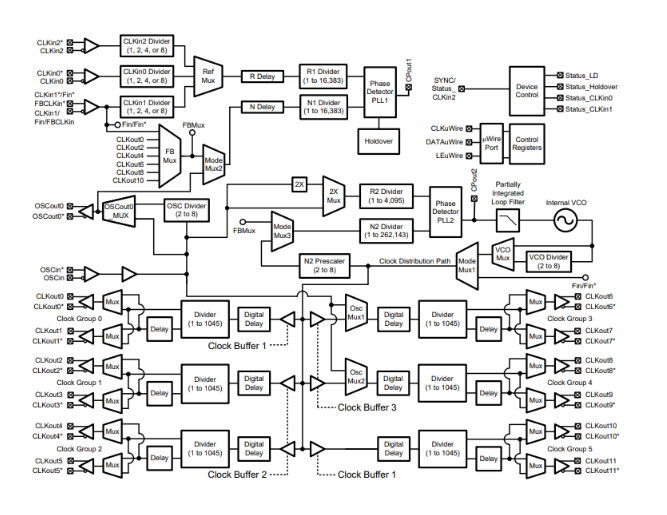
When the transmit/receive sample rate being used by the DRC is set to 200MHz, PLL1 and PLL2 are used together to produce a VCO clock rate of 2400MHz
When a sample rate of 184.32MHz sample rate is set, a VCO clock of 2580.48MHz is used.
In both cases the external 96 MHz VCO is locked to a 10MHz reference using PLL1.
The 96MHz oscillator is multiplied up by PLL2 to the VCO clock rate
The LMK04816 is configured to operated in DUAL PLL mode using the internal VCO. PLL1 locks the 96 MHz oscillator to the reference 10 MHz. The Reference CLKIn is divided by PLL1 R, this is compared to the ClkOut signal divided by PLL1 R. The phase detector compares the resulting 2MHz signals. The CPout1 signal drives the external 96 MHz VCO, which drives the LMK04816 OSCIn signal.
Sample Rate |
Ref CLKin |
PLL1 R |
ClkOut |
PLL1 N |
Phase Det |
OSCIn |
|---|---|---|---|---|---|---|
200 MHz |
10 MHz |
5 |
10 |
5 |
2 MHz |
96 MHz |
184.32 MHz |
10 MHz |
5 |
96 |
48 |
2 MHz |
96 MHz |
PLL2 uses this locked 96 MHz OSCIn signal to produce the VCO frequency.
Sample Rate |
OSCIn |
PLL2 R |
PLL2 pre |
PLL2 N |
Phase Det |
VCO Freq |
|---|---|---|---|---|---|---|
200 MHz |
96 MHz |
2 / 2 |
5 |
5 |
96 MHz |
2400 MHz |
184.32 MHz |
96 MHz |
25 / 2 |
2 |
168 |
7.68 MHz |
2580.48 MHz |
The VCO frequency is then divided down to produce each of the separate clock sources
When operating with a VCO frequency of 2400 MHz
Clock |
Usage |
Divider |
Frequency |
|---|---|---|---|
CLKout0 |
FPGA_CLK |
12 |
200 MHz |
CLKout1 |
CPRI_CLK_CLEAN |
||
CLKout2 |
DB0_RX_REFCLK |
48 |
50 MHz |
CLKout3 |
DB1_RX_REFCLK |
||
CLKout4 |
DB0_TX_REFCLK |
48 |
50 MHz |
CLKout5 |
DB1_TX_REFCLK |
||
CLKout6 |
DB0_DAC_REFCLK |
12 |
200 MHz |
CLKout7 |
DB1_DAC_REFCLK |
||
CLKout8 |
DB0_ADC_REFCLK |
12 |
200 MHz |
CLKout9 |
DB1_ADC_REFCLK |
||
CLKout10 |
REFCLK_OUT |
240 |
10 MHz |
CLKout11 |
CLKOUT |
When operating with a VCO frequency of 2580.48 MHz
Clock |
Usage |
Divider |
Frequency |
|---|---|---|---|
CLKout0 |
FPGA_CLK |
14 |
184.32 MHz |
CLKout1 |
CPRI_CLK_CLEAN |
||
CLKout2 |
DB0_RX_REFCLK |
52 |
49.625 MHz |
CLKout3 |
DB1_RX_REFCLK |
||
CLKout4 |
DB0_TX_REFCLK |
52 |
49.625 MHz |
CLKout5 |
DB1_TX_REFCLK |
||
CLKout6 |
DB0_DAC_REFCLK |
14 |
184.32 MHz |
CLKout7 |
DB1_DAC_REFCLK |
||
CLKout8 |
DB0_ADC_REFCLK |
14 |
184.32 MHz |
CLKout9 |
DB1_ADC_REFCLK |
||
CLKout10 |
REFCLK_OUT |
258 |
10 MHz |
CLKout11 |
CLKOUT |
Worker Properties
The properties of this worker give access to the LMK04816 hardware registers. They written to by the DRC worker. They are not intended to be written by an application.
Utilization
Utilization reporting is not currently implemented.